PSI1250MP IP Brief
Description:
PSI1250MP is a multi-protocol SERDES capable of operating at up to
12.5Gbps. PSI1250MP can provide interfaces for many applications
operating from 9.5Gbps to 12.5Gbps. It also provides interfaces for
applications with 1/2, 1/4 and 1/8 speed. Fig. 1 shows the
simplified top-level block diagram of this module. At the RX side
the serial input data goes through the input stage with linear
equalization. The Clock and data recovery (CDR) circuit receives the
data. It then extracts the clock, and provides the clock and the
retimed data to the de-serializer. The de-serializer converts the
serial data to 8, 10, 16, 20, 32 or 40 bit parallel data with
corresponding rx-clk. A DFE (Decision Feedback Equalization) block
has been implemented in this module, and for the cases where a
higher jitter tolerance is required, it is enabled. A Loss Of Signal
(LOS) detector detects if there are valid data at the input. At the
TX side the serialized data goes through the output driver.
Depending on the application, transmitter can serialize 8, 10, 16,
20, 32 or 40 bit parallel data to a differential serial output. To
further improve the jitter performance there are programmable
pre-emphasis capabilities at the transmitter output stage. In
addition near end serial and far end parallel loopback are
implemented to be able to test the module. To improve signal
integrity the block also includes a calibration circuit providing
control signals to make the transmitter output resistance and the
receiver input resistance within 50Ω±5%.
Features
- A SERDES capable of operating at 9.5-12.5Gbps and 1/2, 1/4, 1/8 speed.
- Jitter generation and jitter tolerance exceed the specifications for many applications such as XFI, 10GBASE_KR, XAUI, RXAUI, SGMII, HRIF, SFI, SATA, SAS, FC and PCIe.
- Serial output driver with calibrated on-chip termination resistor.
- Selectable pre-emphasis level of signal at the output driver.
- Serial input receiver with calibrated on-chip termination resistor.
- Fixed equalization capability at the receiver input.
- Decision Feedback Equalization (DFE)
- Near end serial and far end parallel loopback.
- Loss of signal detector.
- AC JTAG
- Reference clock can be between 80MHz to 800MHz.
- 2 power supplies of 0.9V and 1.2V.
- Only one external component is used (external resistor for termination resistor calibration).
- TSMC 40nm G process.
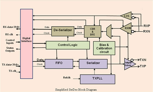
Fig. 1 Simplified block diagram of the top level